Lorem ipsum dolor sit amet, consectetur adipiscing elit. Ut elit tellus, luctus nec ullamcorper mattis, pulvinar dapibus leo.
Lorem ipsum dolor sit amet, consectetur adipiscing elit.

DIVSYS-ICAPE’s fully equipped laboratory offers a complete range of testing services for both bare and assembled printed circuit boards, rework and technical support for Indianapolis PCBA Manufacturing. Our in-house lab inspects the boards we procure to guarantee an exact match with the design file, while offering standalone Indianapolis PCBA Manufacturing services to detect a wide range of manufacturing defects.
PCB Micro-section analysis of the copper and “hole” quality is the most thorough of all of the tests as it allows the examiner to look “inside” the PCB at the quality of the construction, the copper plating, the hole formation, the dielectric separation (which also defines the AC impedance), the lamination process, and the base copper. The IPC has defined 42 different “rejectable” defects that can be seen in one micro section.
Measurement of the surface finish thickness (Au, Ni, Ag, HASL, Sn) by X-Ray Fluorescence on 10 positions
Automatic test to verify net continuity and the absence of shorts on the board.
Mechanical dimension checking.
Measure the glass transition temperature (Tg) of the PCB
Cleanliness Testing is used to measure the amount of ionic contamination left on the surface by the PCB process. A cleanliness tester is filled with a solution of 75% AIPA and 25% DI H20 to dissolve the surface contamination.
The PCB (Or PCBA) is immersed in the solution. This is a Go / No go test that the PCB or PCBA is clean.
The resulting “dirty” solution is measured and converted to a standard using “Equivalent Micro Grams of Sodium Chloride” which is divided by the surface area of the sample to arrive at an ug/in2 or ug/cm2.
The IPC acceptance is <10ug/in2 or < 1.65ug/cm2. Standard cleanliness per IPC TM 650 method 2.3.25.
Separates the different ions to be able to measure the concentration of each of them.
Ion Chromatography per IPC TM 650 method 2.3.28.
Ion Chromatography (IC) is employed when the sample fails the IPC maximum acceptability or if the customer has defined a maximum concentration of a specific ION.
For the Ion Chromatograph, there are two types of ions (Anions and Cations). In PCB fabrication, we are usually only concerned with Anions and hence the measurement standard using equivalent micro grams of chloride.
However, in the no-clean flux of PCBA processing, we also can have Cations. This requires a different measurement system. Both types of ions must be measured and noted for a PCBA.
Measurement of the surface finish thickness (Au, Ni, Ag, HASL, Sn) by X-Ray Fluorescence on 10 positions
Check the integrity of hidden solder connections on the PCBA (such as BGA balls). The PCB can be checked for the alignment of the layers or for voids in the via holes.
When evaluating the integrity of a solder connection, an X-RAY image is invaluable to be able to see the actual connection in a non-destructive fashion.
The X-RAY image can be viewed at various angles to reveal the amount of “attachment between the PCB pads, the component pins and/or the BGA
Examine solder connections on the PCBA or make internal measurements of the PCB’s copper thickness, inner layers, or hole quality.
For solder connections, each location is ground and polished to three depths.
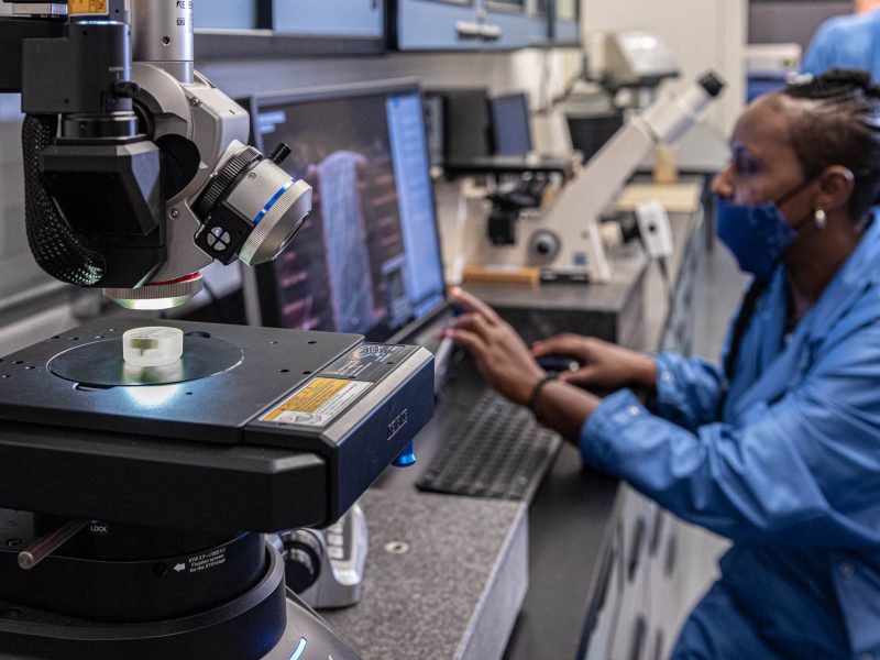
Micro Section Analysis
4K Ultra-High Accuracy Microscope
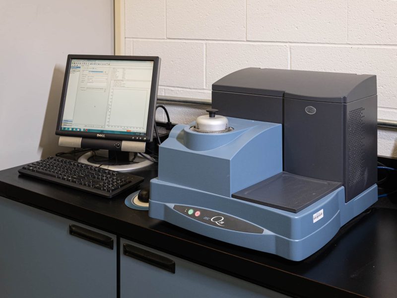
Differential Scanning Calorimeter
Measurement of differential heat flow
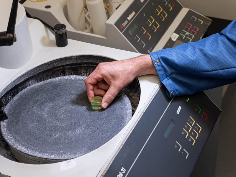
Cross Section
Grinding and polishing
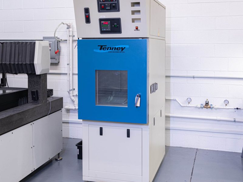
Thermal Shock Chamber
Performs temperature & humidity tests
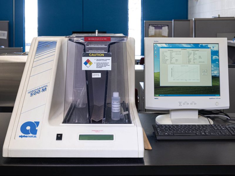
Ionic Contamination
Quick and accurate testing for individual parts, complete assemblies, or small devices
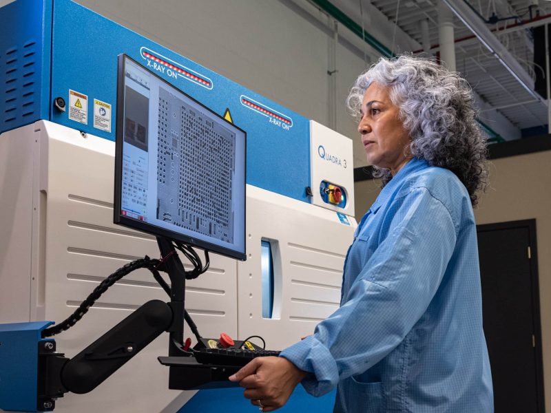
X-Ray Inspection
3D X-ray inspection machine to detect a wide range of manufacturing defects
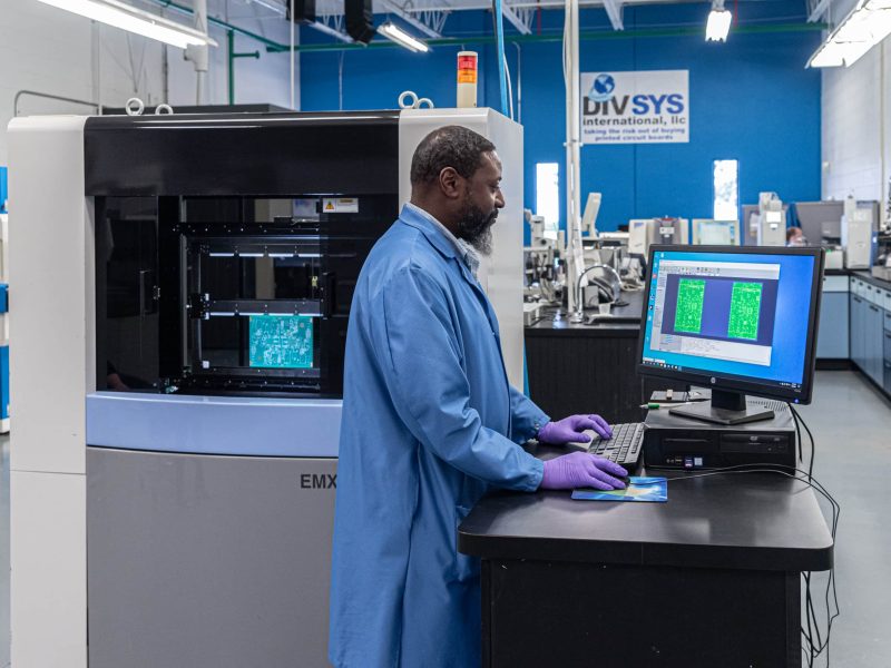
Bare Board Electrical Test
Checks connectivity/isolation
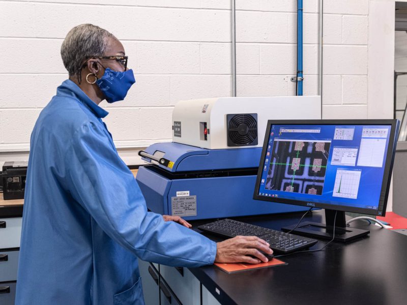
X-Ray Fluorescence
Measurement of thickness of multi-coating elements
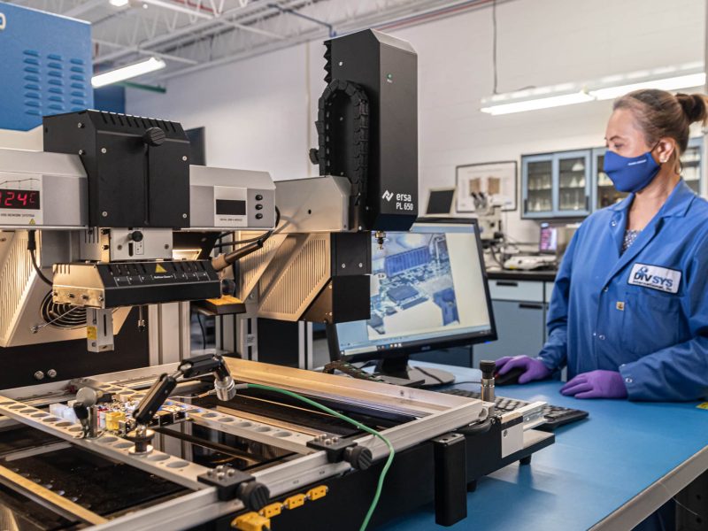
BGA Repair Station
High-performance, universal IR Rework System with semiautomatic component placement
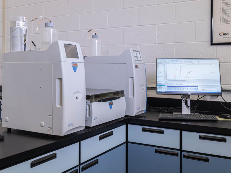
Ion Chromatography
Performs all types of electrolytically generated isocratic and gradient IC separations using conductivity detection
Lorem ipsum dolor sit amet, consectetur adipiscing elit ut elit tellus luctus nec ullamcorper mattis.
Lorem ipsum dolor sit amet
Lorem ipsum dolor sit amet
Lorem ipsum dolor sit amet
Lorem ipsum dolor sit amet


Lorem ipsum dolor sit amet, consectetur adipiscing elit. Ut elit tellus
Lorem ipsum dolor sit amet, consectetur adipiscing elit. Ut elit tellus
Our Quality Policy drives our commitment to continuous improvement and excellence in all Indianapolis PCBA Manufacturing areas—product quality, customer service, technology, and teamwork. It guides both external customers who rely on our services and internal teams working toward shared success.

Our Indianapolis PCBA Manufacturing quality team follows IPC and ISO standards to meet or exceed customer expectations.

We prioritize resources and leadership to enhance our quality management system and customer satisfaction.

Every team member ensures quality control, delivering the required product at the right time with the expected quality level.